Pages

Showing posts with label power. Show all posts

Friday, December 27, 2013

Build a 10 Amp 13 8 Volt Power Supply Circuit Diagram
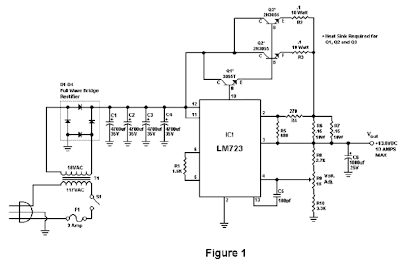
Sometimes amateurs like to home-brew their power supplies instead of purchasing one off the shelf at any of the major ham radio retail dealers. The advantage to rolling your own power supply is that it teaches us how they work and makes it easier to troubleshoot and repair other power supply units in the shack. It should be noted that there is no real cost advantage to building your own power supply unless you can get a large power transformer and heat sink for a super low price. 

Of course rolling our own gives us the ability to customize the circuit and make it even more reliable than commercial units. The circuit in Figure 1 will give us 10 amps (12 amps surge) with performance that equals or exceeds any commercial unit. The circuit even has a current limiting feature which is a more reliable system than most commercial units have. Just like other commercial units, this circuit uses the LM723 IC which gives us excellent voltage regulation. The circuit uses 3 pass transistors which must be heat sinked. Resistor R9 allows the fine tuning of the voltage to exactly 13.8 volts and the resistor network formed by resistors R4 through R7 controls the current limiting. 

The LM723 limits the current when the voltage drop across R5 approaches .7 volts. To reduce costs, most commercial units rely on the HFE of the pass transistors to determine the current limiting. The fault in that system is that the HFE of the pass transistors actually increases when the transistors heat up and risks a thermal runaway condition causing a possible failure of the pass transistors. Because this circuit samples the collector current of the pass transistors, thermal runaway is not a problem in this circuit making it a much more reliable power supply. 

The only adjustment required is setting R9 to the desired output voltage of anywhere between 10 and 14 volts. You may use a front panel mounted 1K potentiometer for this purpose if desired. Resistor R1 only enhances temperature stability and can be eliminated if desired by connecting pins 5 and 6 of IC-1 together. Although it really isn’t needed due to the type of current limiting circuit used, over voltage protection can be added to the circuit by connecting the circuit of Figure 2 to Vout. The only way over voltage could occur is if transistors Q2 or Q3 were to fail with a collector to emitter short. Although collector to emitter shorts do happen, it is more much more likely that the transistors will open up when they fail.

 10 Amp 13.8 Volt Power Supply Circuit Diagram

10 Amp 13.8 Volt Power Supply Circuit Diagram


I actually tested this and purposely destroyed several 2N3055’s by shorting the emitters to ground. In all cases the transistors opened up and no collector to emitter short occurred in any transistor. In any event, the optional circuit in Figure 2 will give you that extra peace of mind when a very expensive radio is used with the power supply. The circuit in Figure 2 senses when the voltage exceeds 15 volts and causes the zener diode to conduct. When the zener diode conducts, the gate of the SCR is turned on and causes the SCR to short which blows the 15 amp fuse and shuts off the output voltage. 

A 2N6399 (Tech America) was used for the SCR in the prototype but any suitable SCR can be used. While over voltage protection is a good idea, it should not be considered a substitute for large heat sinks. I personally feel the best protection from over voltage is the use of large heat sinks and a reliable current limiting circuit. Be sure to use large heat sinks along with heat sink grease for the 2N3055 transistors. I have used this power supply in my shack for several months on all kinds of transceivers from HF, VHF to UHF with excellent results and absolutely no hum. This power supply will be a welcome addition to your shack and will greatly enhance your knowledge of power supplies.

10 Amp 13.8 Volt Power Supply Circuit Diagram2


Parts
R1 1.5K ¼ Watt Resistor (optional, tie pins 6 & 5 of IC1 together if not used.)
R2,R3 0.1 Ohm 10 Watt Resistor (Tech America 900-1002)
R4 270 Ohm ¼ Watt Resistor
R5 680 Ohm ¼ Watt Resistor
R6,R7 0.15 Ohm 10 Watt Resistor (Tech America 900-1006)
R8 2.7K ¼ Watt Resistor
R9 1K Trimmer Potentiometer (RS271-280)
R10 3.3K ¼ Watt Resistor
C1,C2,C3,C4 4700 Microfarad Electrolytic Capacitor 35 Volt (observe polarity)
C5 100 Picofarad Ceramic Disk Capacitor
C6 1000 Microfarad Electrolytic Capacitor 25 Volt (observe polarity)
IC1 LM723 (RS276-1740) Voltage Regulator IC. Socket is recommended.
Q1 TIP3055T (RS276-2020) NPN Transistor (TO-220 Heat Sink Required)
Q2,Q3 2N3055 (RS276-2041) NPN Transistor (Large TO-3 Heat Sink Required)
S1 Any SPST Toggle Switch
F1 3 Amp Fast Blow Fuse
D1-D4 Full Wave Bridge Rectifier (RS276-1185)
T1 18 Volt, 10 Amp Transformer Hammond #165S18 (Tech America 900-5825)
Read More..

Sunday, December 22, 2013

Simple 2304 and 3456 MHz Power Amplifiers Circuit Diagram

This is a Simple 2304 and 3456 MHz Power Amplifiers Circuit Diagram

Circuit-Diagram

Read More..

Tuesday, December 17, 2013

Car Bulb Power Flasher

Derived from the Two-wire Lamp Flasher design, hosted on RED Free Circuit Designs since 1999, this astonishingly simple circuit allows one or two powerful 12V 21W car bulbs to be driven in flashing mode by means of a power MosFet. 
 
Devices of this kind are particularly suited for road, traffic and yard alerts and in all cases where mains supply is not available but a powerful flashing light is yet necessary.

Circuit Diagram:

Power Flash Circuit  Diagram
Car Bulb Power Flasher  Circuit Diagram

Parts Description
R1 6.8K
R2 220K
R3 22K
C1 100uF-25V
C2 10u-25V
D1 1N4002
Q1 BC557
Q2 IRF530
LP1 12V-21W Car Filament Bulb (See Notes)
SW1 SPST Switch (3 Amp minimum)
Notes:
  • Flashing frequency can be varied within a limited range by changing C1 value.
  • As high dc currents are involved, please use suitably sized cables for battery and bulb(s) connections.
Source :  http://www.ecircuitslab.com/2011/06/car-bulb-power-flasher.html
Read More..

Tuesday, October 8, 2013

Dual 20 Watt Audio Power Amplifier

Overture Audio Power Amplifier Series Dual 20-Watt Audio Power Amplifier with Mute and Standby Modes

The LM1876 is a stereo audio amplifier capable of delivering typically 20W per channel of continuous average output power into a 4 or 8 load with less than 0.1% THD+N.

Each amplifier has an independent smooth transition fade-in/out mute and a power conserving standby mode which can be controlled by external logic.

The performance of the LM1876, utilizing its Self Peak Instantaneous Temperature (°Ke) (SPiKe™) protection circuitry, places it in a class above discrete and hybrid amplifiers by providing an inherently, dynamically protected Safe Operating Area (SOA). SPiKe protection means that these parts are safeguarded at the output against overvoltage, undervoltage, overloads, including thermal runaway and instantaneous temperature peaks.

Circuit Diagram

Dual 20-Watt Audio Power Amplifier Dual 20-Watt Audio Power Amplifier Circuit Diagram

Key Specification
THD+N at 1kHz at 2 x 15W continuous average
output power into 4 or 8: 0.1% (max)
THD+N at 1kHz at continuous average
output power of 2 x 20W into 8: 0.009% (typ)
Standby current: 4.2mA (typ)

Applications

  • High-end stereo TVs
  • Component stereo
  • Compact stereo

    Features

  • SPiKe protection
  • Minimal amount of external components necessary
  • Quiet fade-in/out mute mode
  • Standby-mode
  • Isolated 15-lead TO-220 package
  • Non-Isolated 15-lead TO-220 package
  • Wide supply range 20V - 64V

  • Read More..

    Thursday, September 26, 2013

    Super Simple 3 Watt Audio Power Amplifier

    Here is the circuit diagram of superb mini audio power amplifier, That can be power with 4.5 volt dc to 18 volts dc (maximum). This amplifier is based on TDA1015, Product of NXP Semiconductors formerly PHILIPS Semiconductors. The TDA1015 is a monolithic integrated audio amplifier circuit in a 9-lead single in-line (SIL) plastic package. The device is especially designed for portable radio and recorder applications and delivers up to 4 watt in a 4 ohm load impedance. The very low applicable supply voltage of 3,6 V permits 6 V applications.

    3 Watt Audio Power Amplifier circuit project
    3 Watt Audio Power Amplifier circuit schematic
    click on the images to enlarge
    Parts:

    R1330K
    R25.6K
    R34.7R
    C11uF-25V
    C21uF-25V
    C3100pF
    C4100nF-63V
    C5182pF
    C6224pF
    C7100uF-25V
    C8100nF-63V
    C910uF-25V
    C101KuF-25V
    IC1TDA1015

    Applications:
    • In-car use
    • Your own unique application
    • Power amplifier for audio projects
    • For use with portable audio equipment
    • Small but powerful multi-purpose amplifier
    Special features:
    • Low current drain
    • High output power
    • Thermal protection
    • High input impedance
    • Separated preamplifier and power amplifier
    • Limited noise behavior at radio frequencies
    • Single in-line (SIL) construction for easy mounting
    Specification:
    • Quiescent current : 12mA
    • Thermal and short circuit protection
    • Frequency Response : 60Hz - 15Khz
    • Max. output power : 3W (4ohm/12V)
    • Input sensitivity : 20-15mV selectable
    • Power supply : 4.5 - 15V DC @ 400mA
    Read More..

    Sunday, September 1, 2013

    Power Failure and Low Line Signals

    This is a circuit of Power-Fail and Low-Line Signals. This circuit is used to warn the processor when the power failure or a brownout is occurs. The processor will enter a power-down routine, when either of those signals interrupts the processor. Back up important data prior to the POR placing the processor in reset and cease its current  activities are things that the processor do when enter the routine. Here is the circuit.Power-fail comparator is used to create a power-fail signal by monitoring the unregulated DC voltage. The regulator powers both supervisor circuit and the processor by using the the unregulated DC voltage.

    Power-Failure and Low-Line Signals Schematic


    Power-Failure and Low-Line Signals
     The regulator’s output capacitor retains its output voltage, so the unregulated voltage drops before the regulator’s voltage. And also, we can know drop in the regulator’s voltage. The processor can enter its power-down routine prior to being reset, if the power supply voltage were to drop low enough because of Detecting the regulator’s voltage drop.A supervisor provides a low-line signal, which goes active whenever the monitored power supply drops to a level slightly above the reset threshold so the processor can still receive warning of an imminent power failure when there is no access to the unregulated voltage.

    To cause the POR to issue a reset, the processor warned that the power-supply voltage may decrease enough by the low-line signal. To anticipate the POR generating a reset, the processor backs up important data because of power failure  or a brownout.
    Read More..

    Tuesday, April 9, 2013

    Up Down Timer Circuit For A Power Antenna

    This up/down timer circuit was designed to control a power antenna on a late-model vehicle. Normally, this vehicle uses a body computer to control the antenna. However, the person who owned the vehicle wanted to install his own high powered audio stereo system. The original stereo system was tied in with the body computer and this meant that a separate antenna controller was required for the after-market sound system. Also, the power antenna fitted did not have limit switches inside, hence the need for a timed control circuit. Heres how the circuit works. first, assume that the radio antenna control output is not switched on - ie, the radio is switched off.
    In that case, relay RLYC will be off and so relay RLYA will also be off, as is the motor. Conversely, when the radio is switched on, the radio antenna control output line switches to +12V. And when that happens, RLYC closes its contacts and applies power to the circuit. As a result, C2 (330OF) quickly charges via D4, while Q4 is biased on via D5 and R5. This ensures that Q3 and relay RLYB remain off. At the same time, Q2 is is turned on, thus turning on RLYA and applying power to the motor. This drives the antenna in the up direction. During this time, C1 charges via R2.
    Circuit diagram:
    up-down-timer-for -power
    Up/Down Timer Circuit  Diagram
    When the voltage across the capacitor reaches +8.1V, Q1 turns on via ZD1 and so Q2 turns off and switches off the relay - ie, this gives the "up" timeout. Using the values shown for C1, R2 and ZD1 gives an "up" duration of approximately 6 seconds - long enough to fully extend the antenna. D1 discharges C1 (via resistor R1) when the +12V supply is later removed.
    When the radio is switched off (or a CD placed into the stereo unit), the radio antenna control output switches back to 0V. This does several things: first, it turns Q4 off and this allows Q3 to turn on due to the stored charge in C2. Q3 and RLYB now turn on for about six seconds - ie, while C2 discharges via R4 - and this switches power to the motor in the opposite direction to drive the antenna down. Diodes D4 and D5 are there to prevent C2 from discharging back via the circuitry around on Q1 and Q2.
    Author: Peter Howarth - Copyright: Silicon Chip Electronics
    Read More..

    Wednesday, April 3, 2013

    TA8210AH Stereo Car Power Amplifier

    IC TA8210AH By using this you can apply a series of audio power amplifier is the car audio system. In general, all the speakers in the car using a subwoofer speaker, and woofer. Because the car is not big room so the sound is being required is not too high.

    Audio amplifier circuit can work at a minimum voltage 12-volt DC, if supplied under voltage 12-volt amplifier work will be less than the maximum. This amplifier output power up to 200W or 2 x 100W stereo with 8 ohm impedance.


    200W car amplifier schematic

    Part List :

    Resistor

    R1 =1K

    R2 =50K trim

    R3 =1K

    R4 =50K trim

    R5 =680R

    R6 =680R

    R7 =150K

    R8 =2R2

    R9 =2R2

    R10=2R2

    R11=2R2


    Capacitor

    C1 =1uF

    C2 =1uF

    C3 =47uF

    C4 =47uF

    C5 =100n/400V

    C6 =220uF

    C7 =220uF

    C8 =100n/400V

    C9 =100n/400V

    C10=100n/400V


    Intregated Circuit

    IC1=TA8210AH


    Connector

    X2-3=in R

    X2-2=gnd

    X2-1=in L

    X1-1,X1-2=Out R

    X1-3,X1-4=Out L
    Read More..