Showing posts with label diagram. Show all posts
Showing posts with label diagram. Show all posts
Friday, January 10, 2014
Simple Unipolar to Dual Supply Converter Circuit Diagram
Simple Unipolar to Dual Supply Converter Circuit Diagram. 817V The outputs in this circuit are independently variable and can be loaded unsymmetrically. The output voltage remains constant, irrespective of load and changes. By varying potentiometers R2 or R6, the output voltages can be conveniently set. Outputs can be varied between 8 and 17 V, so that the standard ±9, ±12, and ±15 V settings can be made.
Unipolar to Dual Supply Converter Circuit Diagram

This converter is designed for a maximum load current of 1 A and the output impedance of both supplies of 0.35 0. This circuit is not protected against shortcircuits, but uses the protection provided by the de input source. This circuit is ideal for biassing operation amplifier circuits.

Friday, December 27, 2013
Build a 10 Amp 13 8 Volt Power Supply Circuit Diagram
Sometimes amateurs like to home-brew their power supplies instead of purchasing one off the shelf at any of the major ham radio retail dealers. The advantage to rolling your own power supply is that it teaches us how they work and makes it easier to troubleshoot and repair other power supply units in the shack. It should be noted that there is no real cost advantage to building your own power supply unless you can get a large power transformer and heat sink for a super low price.
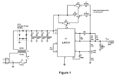
Of course rolling our own gives us the ability to customize the circuit and make it even more reliable than commercial units. The circuit in Figure 1 will give us 10 amps (12 amps surge) with performance that equals or exceeds any commercial unit. The circuit even has a current limiting feature which is a more reliable system than most commercial units have. Just like other commercial units, this circuit uses the LM723 IC which gives us excellent voltage regulation. The circuit uses 3 pass transistors which must be heat sinked. Resistor R9 allows the fine tuning of the voltage to exactly 13.8 volts and the resistor network formed by resistors R4 through R7 controls the current limiting.
The LM723 limits the current when the voltage drop across R5 approaches .7 volts. To reduce costs, most commercial units rely on the HFE of the pass transistors to determine the current limiting. The fault in that system is that the HFE of the pass transistors actually increases when the transistors heat up and risks a thermal runaway condition causing a possible failure of the pass transistors. Because this circuit samples the collector current of the pass transistors, thermal runaway is not a problem in this circuit making it a much more reliable power supply.
The only adjustment required is setting R9 to the desired output voltage of anywhere between 10 and 14 volts. You may use a front panel mounted 1K potentiometer for this purpose if desired. Resistor R1 only enhances temperature stability and can be eliminated if desired by connecting pins 5 and 6 of IC-1 together. Although it really isn’t needed due to the type of current limiting circuit used, over voltage protection can be added to the circuit by connecting the circuit of Figure 2 to Vout. The only way over voltage could occur is if transistors Q2 or Q3 were to fail with a collector to emitter short. Although collector to emitter shorts do happen, it is more much more likely that the transistors will open up when they fail.
10 Amp 13.8 Volt Power Supply Circuit Diagram
I actually tested this and purposely destroyed several 2N3055’s by shorting the emitters to ground. In all cases the transistors opened up and no collector to emitter short occurred in any transistor. In any event, the optional circuit in Figure 2 will give you that extra peace of mind when a very expensive radio is used with the power supply. The circuit in Figure 2 senses when the voltage exceeds 15 volts and causes the zener diode to conduct. When the zener diode conducts, the gate of the SCR is turned on and causes the SCR to short which blows the 15 amp fuse and shuts off the output voltage.
A 2N6399 (Tech America) was used for the SCR in the prototype but any suitable SCR can be used. While over voltage protection is a good idea, it should not be considered a substitute for large heat sinks. I personally feel the best protection from over voltage is the use of large heat sinks and a reliable current limiting circuit. Be sure to use large heat sinks along with heat sink grease for the 2N3055 transistors. I have used this power supply in my shack for several months on all kinds of transceivers from HF, VHF to UHF with excellent results and absolutely no hum. This power supply will be a welcome addition to your shack and will greatly enhance your knowledge of power supplies.

Parts
R1 1.5K ¼ Watt Resistor (optional, tie pins 6 & 5 of IC1 together if not used.)
R2,R3 0.1 Ohm 10 Watt Resistor (Tech America 900-1002)
R4 270 Ohm ¼ Watt Resistor
R5 680 Ohm ¼ Watt Resistor
R6,R7 0.15 Ohm 10 Watt Resistor (Tech America 900-1006)
R8 2.7K ¼ Watt Resistor
R9 1K Trimmer Potentiometer (RS271-280)
R10 3.3K ¼ Watt Resistor
C1,C2,C3,C4 4700 Microfarad Electrolytic Capacitor 35 Volt (observe polarity)
C5 100 Picofarad Ceramic Disk Capacitor
C6 1000 Microfarad Electrolytic Capacitor 25 Volt (observe polarity)
IC1 LM723 (RS276-1740) Voltage Regulator IC. Socket is recommended.
Q1 TIP3055T (RS276-2020) NPN Transistor (TO-220 Heat Sink Required)
Q2,Q3 2N3055 (RS276-2041) NPN Transistor (Large TO-3 Heat Sink Required)
S1 Any SPST Toggle Switch
F1 3 Amp Fast Blow Fuse
D1-D4 Full Wave Bridge Rectifier (RS276-1185)
T1 18 Volt, 10 Amp Transformer Hammond #165S18 (Tech America 900-5825)
R1 1.5K ¼ Watt Resistor (optional, tie pins 6 & 5 of IC1 together if not used.)
R2,R3 0.1 Ohm 10 Watt Resistor (Tech America 900-1002)
R4 270 Ohm ¼ Watt Resistor
R5 680 Ohm ¼ Watt Resistor
R6,R7 0.15 Ohm 10 Watt Resistor (Tech America 900-1006)
R8 2.7K ¼ Watt Resistor
R9 1K Trimmer Potentiometer (RS271-280)
R10 3.3K ¼ Watt Resistor
C1,C2,C3,C4 4700 Microfarad Electrolytic Capacitor 35 Volt (observe polarity)
C5 100 Picofarad Ceramic Disk Capacitor
C6 1000 Microfarad Electrolytic Capacitor 25 Volt (observe polarity)
IC1 LM723 (RS276-1740) Voltage Regulator IC. Socket is recommended.
Q1 TIP3055T (RS276-2020) NPN Transistor (TO-220 Heat Sink Required)
Q2,Q3 2N3055 (RS276-2041) NPN Transistor (Large TO-3 Heat Sink Required)
S1 Any SPST Toggle Switch
F1 3 Amp Fast Blow Fuse
D1-D4 Full Wave Bridge Rectifier (RS276-1185)
T1 18 Volt, 10 Amp Transformer Hammond #165S18 (Tech America 900-5825)
Thursday, December 26, 2013
Part 2 High Voltage Supply Circuit Diagram
This High-Voltage Supply Circuit Diagram uses a transistor oscillator and a voltage multiplier to charge CIO and CI 1 to a high voltage. When the spark gap breaks down, T2 produces a high-voltage pulse via the capacitance discharge of CIO and Cll into its primary. T2 is an auto ignition coil.
Read : High-Voltage Pulse Supply Circuit Diagram
Read : High-Voltage Pulse Supply Circuit Diagram
High-Voltage Supply Circuit Diagram

Wednesday, December 25, 2013
Simple Dc Ac Inverter Circuit Diagram
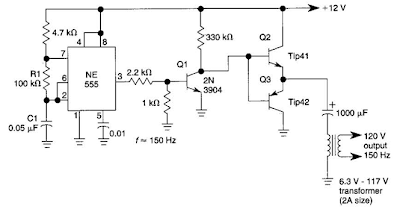
This dc-to-ac inverter is based on the popular 555. A 555 oscillator circuit drives a buffer amplifier consisting of Ql, Q2, and Q3.
The circuit operates at 150 to 160 Hz. Tl can be a 6.3-V or 12.6-V filament transformer as applicable.The frequency can be changed by changing the values of Rl and/or Cl.
Simple Dc/Ac Inverter Circuit Diagram
Monday, December 23, 2013
Simple RF Transmitter for PIR Sensors Circuit Diagram
This is the Simple RF Transmitter for PIR Sensors Circuit Diagram.

Sunday, December 22, 2013
Simple 2304 and 3456 MHz Power Amplifiers Circuit Diagram
This is a Simple 2304 and 3456 MHz Power Amplifiers Circuit Diagram

Thursday, December 19, 2013
Simple Automatic Water Pump Controller Circuit Diagram
Simple Automatic Water Pump Controller Circuit Diagram is a series of functions to control the Automatic Water Pump Controller Circuit in a reservoir or water storage. As the water level sensor made with a metal plate mounted on the reservoir or water tank, with a sensor in the short to create the top level and a detection sensor for detecting long again made the lower level and ground lines connected to the bottom of reservoirs or reservoir.
The series of automatic water pump controller is designed with 2 inputs NOR by 4 pieces and relay that is activated by the transistor. Automatic water pump circuit requires +12 VDC voltage source and can be used to control the water pump is connected to AC power . Here is the complete series of pictures.
Automatic Water Pump Controller Circuit Diagram

working principle series of automatic water pump controller above is. At the time the water level is below both sensors, the output IC1C (pin 10) will be LOW, Kemudin when the water began to touch the lower level sensor, the output IC1C (pin10) remains LOW until the water touches the sensor level above, then the output IC1C (pin 10) going HIGH and active relay through Q1 and turn on the water pump to meguras reservoir.
At the muli down and water level sensors for water untouched MKA IC1C output (pin 10) remains HIGH until the new water untouched semuasensor IC1C output (pin 10) LOW and water pump died. The series of automatic water pump controller is equipped with SW1 which serves to reverse the logic of drains (the output of IC1C) and the concept of water supplied (output dri IC1D).
When SW1 is connected to IC1D the water pump will turn on when the water does not touch all the sensors and will die when all the sensors tesentuh water. Automatic water pump controller can be used to fill or drain the water according to which mode is selected via SW1.
List Component Automatic Water Pump Controller
R1 = 15K
R2 = 15K
R3 = 10K
R4 = 1K
D1 = LED
D2 = 1N4148
Q1 = BC337
IC1 = 4001
SW = SPDT Switches
Relay RL1 = 12V
Thursday, October 10, 2013
2004 Chevrolet Corvette Coupe 350 Wiring Diagram
 |
| 2004 Chevrolet Corvette Coupe 350 Wiring Diagram |
The Part of 2004 Chevrolet Corvette Coupe 350 Wiring Diagram:power distribution, fuse block, turn
signal, switch signal, ctrl module, panel cluster, power distribution schematic, multifunction turn signal lever, underhood fuse block, cruise control switch, powertrain control module, serial data, sedel data secondary, throttle actuator control module, instrument panel cluster, powertrain control module.
signal, switch signal, ctrl module, panel cluster, power distribution schematic, multifunction turn signal lever, underhood fuse block, cruise control switch, powertrain control module, serial data, sedel data secondary, throttle actuator control module, instrument panel cluster, powertrain control module.
Saturday, October 5, 2013
LOW NOISE WHITE LED DRIVER SYSTEM ELECTRONIC DIAGRAM

LOW NOISE WHITE LED DRIVER SYSTEM ELECTRONIC DIAGRAM
The LM3570 evaluation board has a chip enable pin (active high logic) as well as a PWM (active high logic) pin which allows current sources to be turned on and off without completely disabling the part..The LM3570 is capable of supplying up to 80mA of current split between the regulated current sources and VOUT. The LM3570 comes in National’s LLP-14 package.
Friday, October 4, 2013
YAMAHA R5C 350 ELECTRONIC DIAGRAM

YAMAHA R5C 350 ELECTRONIC DIAGRAM
It shows the connection between the parts such as the front flasher light, rear flasher light, flasher relay, battery, fuse, tail light, stop light, rear flasher light, rear stop switch, neutral switch, front stop switch, AC generator, coil, rectifier, regulator, horn, head light, tachometer, speedometer, high beam indicator light, rear flasher, front flasher, and many more.
Tuesday, September 24, 2013
MP3 FM Transmitter Circuit Diagram
Heres a simple VHF FM transmitter that could be used to play audio files from an MP3 player or computer on a standard VHF FM radio. The circuit use no coils that have to be wound. This FM transmitter can be used to listen to your own music throughout your home. When this FM transmitter used in the car, there is no need for a separate input to the car stereo to play back the music files from your MP3 player.
Project image :
To keep the circuit simple as well as compact, it was decided to use a chip made by Maxim Integrated Products, the MAX2606 [1]. This IC from the MAX2605-MAX2609 series has been specifically designed for low-noise RF applications with a fixed frequency. The VCO (Voltage Controlled Oscillator) in this IC uses a Colpitts oscillator circuit. The variable-capacitance (varicap) diode and feedback capacitors
for the tuning have also been integrated on this chip, so that you only need an external inductor to fix the central oscillator frequency.
for the tuning have also been integrated on this chip, so that you only need an external inductor to fix the central oscillator frequency.
t is possible to fine-tune the frequency by varying the voltage to the varicap. Not much is demanded of the inductor, a type with a relatively low Q factor (35 to 40) is sufficient according to Maxim. The supply voltage to the IC should be between 2.7 and 5.5 V, the current consumption is between 2 and 4 mA. With values like these it seemed a good idea to supply the circuit with power from a USB port.
Circuit diagram: 
Resistors (all SMD 0805)
R1,R2 = 22kΩ
R3 = 4kΩ7
R4,R5 = 1kΩ
R6 = 270Ω
P1 = 10kΩ preset, SMD (TS53YJ103MR10 Vishay Sfernice, Farnell # 1557933)
P2 = 100kΩ preset, SMD(TS53YJ104MR10 Vishay Sfernice, Farnell # 1557934)
Capacitors (all SMD 0805)
C1,C2,C5 = 4μF7 10V
C3,C8 = 100nF
C4,C7 = 2nF2
C6 = 470nF
Inductors
L1 = 390nF, SMD 1206 (LQH31HNR39K03L Murata, Farnell # 1515418)
L2 = 2200Ω @ 100MHz, SMD, common-mode choke, 1206 type(DLW31SN222SQ2L Murata, Farnell #1515599)
Semiconductors
IC1 = MAX2606EUT+, SMD SOT23-6 (Maxim Integrated Products)
Miscellaneous
K1 = 3.5mm stereo audio jack SMD (SJ1-3513-SMT
CUI Inc, DIGI-Key # CP1-3513SJCT-ND)
K2 = 5-pin header (only required in combination with 090305-I pre-emphasis circuit)
K3 = USB connector type A, SMD (2410 07 Lumberg, Farnell # 1308875)
A common-mode choke is connected in series with the USB connections in order to avoid interference between the circuit and the PC supply. There is not much else to the circuit. The stereo signal connected to K1 is combined via R1 and R2 and is then passed via volume control P1 to the Tune input of IC1, where it causes the carrier wave to be frequency modulated. Filter R6/C7 is used to restrict the bandwidth of the audio signal. The setting of the frequency (across the whole VHF FM broadcast band) is done with P2, which is connected to the 5 V supply voltage.
The PCB designed uses resistors and capacitors with 0805 SMD packaging. The size of the board is only 41.2 x 17.9 mm, which is practically dongle-sized. For the aerial an almost straight copper track has been placed at the edge of the board. In practice we achieved a range of about 6 metres (18 feet) with this. There is also room for a 5-way SIL header on the board. Here we find the inputs to the 3.5 mm jack plug, the input to P1 and the supply voltage. The latter permits the circuit to be powered independently from the mains supply, via for example three AA batteries or a Lithium button cell. Inductor L1 in the prototype is a type made by Murata that has a fairly high Q factor: minimum 60 at 100 MHz.
PCB Layout :
Take care when you solder filter choke L2, since the connections on both sides are very close together. The supply voltage is connected to this, so make sure that you don’t short out the USB supply! Use a resistance meter to check that there is no short between the two supply connectors before connecting the circuit to a USB port on a computer or to the batteries.
P1 has the opposite effect to what you would expect (clockwise reduces the volume), because this made the board layout much easier. The deviation and audio bandwidth varies with the setting of P1. The maximum sensitivity of the audio input is fairly large. With P1 set to its maximum level, a stereo input of 10 mVrms is sufficient for the sound on the radio to remain clear. This also depends on the setting of the VCO. With a higher tuning voltage the input signal may be almost twice as large (see VCO tuning curve in the data sheet). Above that level some audible distortion becomes apparent. If the attenuation can’t be easily set by P1, you can increase the values of R1 and R2 without any problems.
Measurements with an RF analyzer showed that the third harmonic had a strong presence in the transmitted spectrum (about 10 dB below the fundamental frequency). This should really have been much lower. With a low-impedance source connected to both inputs the bandwidth varies from 13.1 kHz (P1 at maximum) to 57 kHz (with the wiper of P1 set to 1/10). In this circuit the pre-emphasis of the input is missing. Radios in Europe have a built-in de-emphasis network of 50 μs (75 μs in the US). The sound from the radio will therefore sound noticeably muffled. To correct this, and also to stop a stereo receiver from mistakenly reacting to a 19 kHz component in the audio signal, an enhancement circuit Is published elsewhere in this issue (Pre-emphasis for FM Transmitter, also with a PCB). Author: Mathieu Coustans, Elektor Magazine, 2009
Notice. The use of a VHF FM transmitter, even a low power device like the one described here, is subject to radio regulations and may not be legal in all countries.
Source :http://fmtvguide.blogspot.com
Saturday, September 21, 2013
2000 Chevrolet 2500 Express Van Wiring Diagram
 |
| 2000 Chevrolet 2500 Express Van Wiring Diagram |
The Part of 1957-58 Dodge 4-Way Power Seat Wiring Diagram: power distribution, relay center,
ignition switch, fusible link, red wire, yellow wire, fuse block, starter motor, solenoid, generator, battery, black wire, fuse relay center, neutral position switch, starter relay, solenoid contacts, generator, black wire
ignition switch, fusible link, red wire, yellow wire, fuse block, starter motor, solenoid, generator, battery, black wire, fuse relay center, neutral position switch, starter relay, solenoid contacts, generator, black wire
Friday, September 20, 2013
1988 Ford F150 Wiring Diagram
 |
| 1988 Ford F150 Wiring Diagram |
(click for full size image)
The Part of 1988 Ford F150 Wiring Diagram:fuse link, black wire, electronic eigne control, start, starter relay, batterey, starter motor, radio mouse capacitr, starter igmition, instrument cluster, charger, indicator lamp, fuse panel, charge power distribution.
Tuesday, June 4, 2013
Yamaha Wr450f Trac Cabel Wiring Diagram Manual Service

Trailer Wiring Diagram Trailer Plug Diagram.

Post It But I Ll Try To Diagram It Here.

The Following Schematic Shows A Typical Diagram Schematic Of Polaris.

Wiring Diagram.

Typical 7 Way Trailer Wiring Diagram Circuit Schematic.

We Recommend A Truck Or Suv With A V 8 Engine For Best Towing.

Anti Theft System And Alarm Circuit Wiring Diagram Circuit Schematic.

Yamaha Wr450f S 2 Trac Cabel Wiring Diagram For Manual Service.

Here Is A Typical Schematic Of Bentley Parrot 3200 Ls Wiring Diagram.

Wiring Diagram.
Thursday, May 30, 2013
Engine Wiring Diagram Wireprestolite Wire

How Does My Ignition System Work Coil Distributor And Cap Rotor.

Engine Wiring Diagram 2 How To Wire A Car Prestolite Wire.

Find More Info 1999 Chevrolet Corvette Fuel Pump Relay Control.

The Following Schematic Shows The Honda Cb750 Sohc Engine Diagram.

1996 Mazda Millenia Wiring Diagram And Electrical System.

Ktm 250 525 Sx Mxc Exc Electrical System And Wiring Diagram.

Find More Information About The Volvo Wiring Diagram S40 V40 2004.

Alternative Offroad Lights Or Accessory Wiring Diagram Using A Relay.

Tda1562q Car Amplifier Circuit Diagram.

1957 Ford Fairlane 500 Wiring Diagram And Electrical System Schematic.
Sunday, May 26, 2013
Honda Civic Hatchback Radiator Parts Diagram

Eddie Van Halen S Frankenstrat Pictured With 22 Fret Kramer Neck.

Stratocaster Guitar Set Up Wiring Diagram Ideas Around Electrical.

Bass Sensor Wiring Instruction Orange Lead Is Electrical Hot.

Amplifier Circuit Diagram.

With 1 Volume Guitar Wiring Diagram Automotive Wiring Diagrams.

Dimarzio 4 Wire Humbucker Color Codes Wiring Shown For Standard.

Honda Civic Hatchback Fan Radiator Parts Diagram 02 03.

Here Is A Very Good Diagram Of How To Wire One Pickup For Coil Taps.

Before I Start With The Guitar Capacitors I D Like To Apologize Up.

Guitar Electroncis Wiring Diagram Logo Jpg.
Wednesday, April 10, 2013
1982 Jeep CJ 5 Wiring Diagram
 |
| 1982 Jeep CJ-5 Wiring Diagram |
The Part of 1982 Jeep CJ-5 Wiring Diagram: dimmer switch, headlamp, turn indicator, ignition switch,
voltmeter, pressure gage, fuse block, dome lamp, light switch, turn signal flasher, voltage regulator, temp gage sender, tachometer, park brage switch, brake warning indicator, backup lamps
voltmeter, pressure gage, fuse block, dome lamp, light switch, turn signal flasher, voltage regulator, temp gage sender, tachometer, park brage switch, brake warning indicator, backup lamps
Sunday, April 7, 2013
Fuse Box Toyota 1985 Celica Diagram
Fuse Box Toyota 1985 Celica Diagram - Here are new post for Fuse Box Toyota 1985 Celica Diagram.


Fuse Panel Layout Diagram Parts: defogger relay, gauge, radio, ECU, ignition system, dome, cigar lgihter, charge light relay, wiper/washer, stop lamp, dimmer relay, headlight relay, Charge, engine, hazzard-horn, tail light, headlamp, tail light relay, main relay, ignition key light relay.
Read More..
Fuse Box Toyota 1985 Celica Diagram


Fuse Panel Layout Diagram Parts: defogger relay, gauge, radio, ECU, ignition system, dome, cigar lgihter, charge light relay, wiper/washer, stop lamp, dimmer relay, headlight relay, Charge, engine, hazzard-horn, tail light, headlamp, tail light relay, main relay, ignition key light relay.
Subscribe to:
Posts (Atom)